Erik Hosler Shares Insights About Fabrication at the Edge of Precision Patterning for Quantum

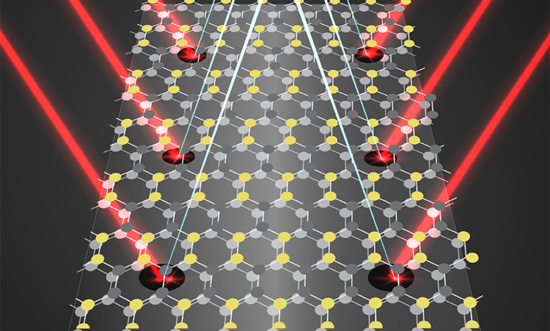
Quantum computing has forced the semiconductor world to confront an uncomfortable truth. Once tolerable imperfections are now unacceptable. In the classical domain, engineers had room to hide variability. Clever design and error margins could absorb minor deviations. In quantum physics, there is no such luxury. Patterning must approach flawless execution. It is because even microscopic irregularities can disrupt quantum states, introduce stochastic noise, and break coherence across arrays. During a panel at the SPIE Advanced Lithography symposium, Erik Hosler, a panelist with a focus on variability and lithographic precision in quantum platforms, captured the dilemma with a mix of pragmatism and ambition.
It is not about polishing an already smooth surface. It is about redefining what acceptable means in a landscape where the smallest defect can collapse an entire operation. For engineers working at the edge of feasibility, the demands of quantum are forcing new conversations about control, consistency, and whether traditional metrics still apply. Fabrication now defines the limits of the quantum roadmap.
Why Quantum Chips Are Less Forgiving
The margin of error for quantum devices is vanishingly small. These systems rely on qubits that maintain a precise state of superposition or entanglement. It must often happen at cryogenic temperatures and across extended operations. A single inconsistency, such as a bump in a gate, a charge trap at an interface, or a sliver of line edge roughness, can result in decoherence, gate error, or complete system failure.
It stands in contrast to classical integrated circuits, which are built to tolerate variation. For years, CMOS scaling allowed engineers to work around imperfections through redundancy, logic correction, and statistical averaging. Transistors could vary slightly in size or performance and still function reliably.
Quantum computing removes that safety net. It demands exact spacing between elements, consistent coupling strength, and predictable physical behavior across every device on the chip. Defects cannot be averaged out. They must either be eliminated or understood well enough to neutralize their effect.
That pressure puts significant demands on lithography, etch uniformity, and interface chemistry. The materials must not only support qubit operation but must also do so uniformly across complex, often multi-layered device architectures. Unlike traditional chips, quantum systems are still largely custom-built, which only amplifies the challenge of achieving consistency.
Striving for Perfect, Settling for Scalable
This challenge was acknowledged directly in the SPIE panel session. “We’d like to see perfection in our patterning, but we’ll settle for striving for perfection,” Erik Hosler says. It is a dry observation, but a revealing one. It captures both the impossibility of achieving ideal patterning and the absolute necessity of pushing as close to it as possible. For quantum systems, the cost of imperfection is too high to ignore. So even if perfection is unattainable, striving for it becomes the only viable strategy.
This effort means pushing lithographic precision beyond conventional standards. It requires controlling variability not just in mask production, but in resist development, etch conditions, and interface chemistry. It also demands extending metrology into regimes where atomic-scale measurement is essential.
Quantum developers do not have the option of working around defects. They must either prevent them or correct them in ways that do not degrade performance. It includes improving the deposition of superconducting materials, reducing interface roughness, and understanding how every nanometer of deviation affects system behavior.
Hosler’s quote reflects a broader truth. The path forward depends less on breakthroughs and more on relentless refinement. Progress is unlikely to come from a single innovation. It will come from tighter tolerances and cleaner control at every step.
Edge Variability and the Limits of Control
Among the many patterning challenges in quantum fabrication, edge variability is one of the most difficult to eliminate. Line edge roughness, overlay misalignment, and etch bias can all introduce inconsistencies at the sub-nanometer scale. In a traditional chip, these irregularities might degrade performance slightly. In a quantum device, they can shift resonance frequencies, alter gate thresholds, or create crosstalk between components.
It becomes especially problematic in large 2D arrays of qubits, where uniformity across the entire chip is essential. A quantum computer with hundreds of qubits must treat each one identically. Otherwise, calibration becomes unmanageable and error correction fails.
In 3D integration, where control wiring is routed vertically through stacked layers, edge placement errors become even harder to detect and correct. Variability between layers can introduce timing mismatches and distort the magnetic field distribution. It leads to performance loss that is difficult to trace and even harder to eliminate.
Control in this environment means more than just accuracy in one layer. It means maintaining consistent behavior across every layer, even under thermal cycling and environmental shifts. It is what makes quantum fabrication not just demanding, but fundamentally fragile.
The SPIE Connection Between Lithography and Quantum
The SPIE Advanced Lithography symposium has long been a forum for addressing patterning, resist chemistry, and metrology. These topics now carry new weight in quantum development. Take resist behavior, for example. Chemically amplified resists used in EUV lithography are prone to stochastic defects. These are small molecular inconsistencies that cause incomplete development or dissolve. In classical devices, they lower the yield. In quantum systems, they alter the physics of the device.
Metrology is developing to meet this demand. Traditional techniques may not suffice when edge placement and material consistency must be tracked at the atomic level. More advanced tools like scanning probe microscopy and cryogenic electron tomography are now required to capture the minute details that influence quantum behavior.
The demands of quantum are also pushing the limits of what EUV lithography can reliably deliver. Wavelength, resist sensitivity, and exposure stability now determine the minimum features achievable in control gates, couplers, and qubit arrays. The message from SPIE is clear. The most advanced lithography techniques are not optional in quantum hardware. They are the starting point.
Closer to Perfect, One Layer at a Time
There is no escaping the fact that quantum fabrication is difficult. But difficulty alone is not the barrier. The challenge is repeatability. Engineers do not need to eliminate all variability. They need to reduce it enough so that systems behave predictably from wafer to wafer.
That is why striving for perfection is more than a goal. It becomes a process. Every mask correction, etch recipe, and layer alignment must contribute to a final product that performs reliably across many devices.
The return on this effort is real. As patterning improves, usable qubits increase. Systems become easier to calibrate. Reliability improves. And the pathway to scale becomes more realistic. The future of quantum computing will not be determined solely in theory. It will be shaped by the engineers in cleanrooms who know that even if perfection is unattainable, there is no excuse for not moving toward it. That movement will happen one layer at a time.